 Afrikaans
 Azərbaycan
 Bosanski
 Čeština
 Dansk
Dansk Deutsch
 English
 Español
 Filipino
 Français
 Hrvatski
 Indonesia
 Italiano
 Magyar
 Melayu
 Nederlands
 Norsk
Norsk Oʻzbek
 Polski
 Português
 Română
 Slovenčina
 Slovenščina
 Suomi
Suomi Svenska
 Tiếng Việt
 Türkçe
 Ελληνικά
 Беларуская
 Български
 Русский
 Српски
 Українська
 עברית
עברית اردو
اردو العربية
 پښتو
پښتو فارسی
فارسی አማርኛ
አማርኛ मराठी
मराठी বাংলা
বাংলা தமிழ்
தமிழ் ไทย
ไทย မြန်မာ
 한국어
한국어 中文
中文 日本語
日本語

இந்த வலைப்பதிவு, உலகில் அதிகம் முன்னேறிய செயலி தொழில்நுட்பங்களில் ஒன்றான 5nm மற்றும் அதற்கும் குறைவான செயலிகள் பற்றிய விரிவான பார்வையை வழங்குகிறது. கடந்த கால வளர்ச்சி, இந்த தொழில்நுட்பத்தின் உடனடிப் பிரச்சனைகள், நடைமுறை செயலி வகைகள், சமீபத்திய சிப்சில் பயன்படுத்தப்படும் புதுமையான பொருட்கள் — இவை அனைத்தும், வெறும் இலக்குகளைத் தாண்டி, தொழில்நுட்பத்தின் இதயத்தில் சென்று விளக்கப்படுகின்றன. 5nm மற்றும் குறைவான செயலிகள் திறன் மற்றும் செயல்திறனை எப்படி அதிகமாக்குகின்றன என்பதையும், எதிர்கால 2nm தொழில்நுட்ப வளர்ச்சியை எப்படி வடிவமைக்கின்றன என்பதையும் கைபேசியிலும், கணினிகளில் கூடவும் காட்டுகிறது. பயனாளர்களுக்கு இந்த மாற்றங்கள் என்ன பயன்பாடு, சூழ்நிலை விழுந்தால் என்ன செய்ய வேண்டும் என்பதாக முடிவில் செயல்பட வேண்டிய அடுத்த கட்டங்களை வழங்குகிறது.
சுருக்கம்: 5nm மற்றும் குறை செயலி வளர்ச்சி வரலாறு
அரைமின்சாரத் துறையின் இலக்கானே — சிறிதாக, வேகமாக, மிக எளிதாக செயலிகளைக் கொண்டு வருவது. இதன் மிக முக்கிய புதிய கட்டம்: 5nm மற்றும் குறைவான செயலி விகிதம். இவற்றில், transistor அளவுகள் நானோமீட்டர் அளவிற்கு குறையும்போது, செயலி திறன், காலத்துக்கு செலையும் மிக அதிகமாகிறது. ஆனால், இவற்றில் இயற்கை science மற்றும் engineering வேட்கைகள் அதிகமாக பொதிந்துள்ளன.
| வருடம் | தொழில்நுட்பம் | அம்சங்கள் |
|---|---|---|
| 2018 | 7nm | முதல் வணிக ரீதியான செயலிகள், மேம்பட்ட செயல்திறன் |
| 2020 | 5nm | Transistor அடர்த்தி மிக அதிகம், குறைந்த சக்தி தேவை |
| 2022 | 4nm/3nm | வெப்ப மாற்றம், திறன் அதிகரிப்பு |
| எதிர்காலம் | 2nm மற்றும் கீழ் | ஆராய்ச்சி, Quantum விளைவுகள் |
5nm மற்றும் குறை செயலி தொழில்நுட்பம், 7nm முதல் 5nm-க்கு வந்தபோது மிக முக்கிய மாற்றங்கள் வந்தன: transistor அடர்த்தி உயர்ந்து, எலக்ட்ரிகல் சக்தி குறைந்தது. இதனை lithografi வளர்ச்சி, புதிய material கண்டுபிடிப்பு, architecture சொந்த முறைகள் இயக்கியவை. இது சாதாரண ‘சின்னம்’ தான் என்றால் தவறு — தொழில்நுட்பம் முழுமையாக மாற்றப்பட்டது.
வரலாற்று மாற்றங்கள்
- 1950கள்: முதற் transistor கண்டுபிடிப்பு, IC உருவாக்கம்
- 1965: Moore’s Law – transistor அபிவிருத்தி தன்மை
- 2000கள்: 90nm, 65nm, 45nm குறைவு மோசமாக
- 2010கள்: FinFET transistor, 22nm, 14nm, 10nm தரம்
- 2018: 7nm செயலிகள் வணிக உலகம் அடைந்தன
- 2020: 5nm தொழில்நுட்பம் பயன்பாட்டில் பெருகியது
அந்த வகை transistor அளவு குறையும்போது quantum physics விளைவுகள் முக்கியமானது. transistor நடத்தை கணிக்க முடியாமல் போகிறது; வெப்பங்களும், சக்தி அளவுகளும் முற்றிலும் complex-ஆகின்றன. Engineers, scientists, புதுமையான material-கள், design, fabrication method-கள் கொண்டு இவை எல்லை மீறி பயணித்திருக்கின்றனர்.
சிறிதாக இடம், குறைந்த சக்தி, அதிக செயலி திறன் — 5nm மற்றும் குறை தொழில்நுட்பங்கள் செயற்கை நுண்ணறிவு, machine learning, high performance computing-க்கு புதிய வாயிலாக உள்ளன. எதிர்கால வளர்ச்சி இனி electronics-க்கு மட்டும் இல்லாமல், உங்கள் வாழ்க்கைக்கும் திசை மாற்றும்!
5nm மற்றும் குறை: உட்பட இயற்கை வரம்புகள்
5nm அல்லது அதுக் கீழ் transistor அளவில் engineering, material science-ல் பெரும் அட்டகாசங்கள் உள்ளன. இது, nano அளவில் செய்யும் transistor fabrication quantum physics-ல் ‘tunneling’ effect போன்ற பிரச்சனைகள் உண்டாக்குகிறது. Silikon உடன் வரம்புகள் வந்ததும், alternatif material, architecture நாடுதல் அவசியமாகிறது.
Designers, chip makers, 5nm மற்றும் குறை வடிவங்கள் கிடைக்கும் பிரச்சனைகளுக்கு modern வாயிலாக gate-all-around, novel dielectric material, short channel length, transistor structures ஆகியவற்றைச் சோதிக்கின்றனர். Moore’s Law தொடர்வது, அளவை குறைத்து சிறந்த செயலி செய்யும் தூரம், இவற்றைச் சாரும்.
5nm மற்றும் அதற்கும் குறைவான செயலிக்கான முக்கிய engineering சிக்கல்கள்
| சிக்கல் | விளக்கம் | புதிய தீர்வு |
|---|---|---|
| Quantum tunneling | Electron முக்கியமான barrier-ஐ கடந்துவிடுதல் | மாற்றிய dielectrics, transistor design enhancements |
| Power density மேலோட்டம் | சில்லறை transistor அதிகம், இடம் குறைந்து | 3D chips, advanced thermal management |
| Production flaws | Nanometer அளவு fabrication சிக்கல்கள் | EUV lithography, error correction methods |
| Material limits | Silicon-ஐ பயன்படுத்தும் physical bounds | Novel semiconductor materials (e.g. gallium nitride) |
இப்போது, 5nm மற்றும் குறை engineering barriers, சரியான material, chip layout, fabrication process வைத்து தாண்ட முயற்சிக்கின்றனர். இந்த முனையில் — தொழில்நுட்பங்களின் வருங்காலம் இவை எவ்வளவு திறனாக விலக்கப்படுகிறது என்பதில்தான் உள்ளது.
உட்பட இயற்கை சிக்கல்கள்
- Quantum tunneling, leakage
- Higher power draw, heat output
- Fabrication variability, nano level errors
- Material science constraints (silicon limits)
- Transistor reliability and lifespan
- High cost manufacturing methods
மைக்ரோ கட்டமைப்புகள்
மைக்ரோ கட்டமைப்புகள் 5nm மற்றும் குறை-இல் முக்கிய பங்கு வகிக்கின்றன: transistor geometry, arrangement, direct impact on performance, power, reliability. 2D structures-ல் limitations வந்ததும், FinFET and GAAFET போன்ற 3D transistor-கள் தற்போது முக்கிய பங்கு தருகின்றன.
Chip-இல் internal component placement, wire length optimization — signal delay குறைக்கும், overall performance மேம்படுத்தும்! இது advanced layout algorithm-க்கும், architecture-conscious design-க்கும் வழிகாட்டுகிறது. ஒரு சொன்னமொழி:
5nm மற்றும் அதற்கும் குறைவான chip வகையில், transistor மட்டுமல்ல; chip wiring, overall architecture optimization நிதானமானது. வெற்றிகரமான compact design-கள் மிகச்சிறந்த செயல்திறன் மற்றும் குறைந்த சக்தி கருதுகின்றன.
வெப்ப மேலாண்மை
வெப்ப மேலாண்மை 5nm மற்றும் குறை chip fabrication-ல் மிக முக்கிய engineering fight. பெரிய transistor density — அதிக heat. இதனால் performance குறையும், reliability குறையும், worst-case-இல் permanent damage வரலாம். Heat management essential!
Advanced heat spreaders, liquid cooling, chip-integrated thermal sensors, dynamic frequency scaling, voltage modulation — இவை அனைத்தும் high-performance chip-க்கு பூங்காற்றாகும். Thermal innovations இன்றி, chip longevity, user-experience நிச்சயமாக பாதிக்கப்படும்.
செயலி அமைப்புகள்: மாறும் முறைகள்
செயலி architecture என்பது — chip எப்படி வடிவமைக்கப்படுகிறது, இயக்கப்படுகிறது என்பதை நிர்ணயிக்கும். 5nm மற்றும் குறை இந்தப் புதிய அளவு, architecture-யில் பெரிய impact ஆடுகிறது. மரபான வகைகளிலிருந்து, புதிய design-முள்ள modern chip capabilities-க்கு முன்னுரிமை தருகின்றன.
Parallellism, energy efficiency, application targeting: multiple core CPUs (multi-tasking), GPU (parallel graphics & AI), FPGA (hardware-level customization), ASIC (specialized high-performance) — உங்களுக்கான சிறந்த choosing!
சிறந்த செயலி architectures
- x86: போர்வன desktop, laptop, CISC architecture-யில் முக்கியமானது
- ARM: Mobile, embedded devices-ஐள்ளுகின்ற RISC, lesser-power architecture
- GPU: Parallel calculation & graphics processing, AI, games
- FPGA: Hardware reprogrammable, custom logic
- ASIC: Ultra-specific, efficient chip design (one task for fastest performance)
Architecture-யில் hardware மட்டுமல்ல, software compatibility, development convenience என இரண்டும் கேட்கிறது. 5nm மற்றும் குறை-இல், physics limits touched; optimization-ன் தீவிரம் அதிகரிக்கிறது. Performance, power-saving, future-proof ஊக்குவிக்க architects நாடுகின்றனர்.
| Arch | விசேஷங்கள் | கூடுதல் பயன்பாடுகள் |
|---|---|---|
| x86 | High performance, vast software base | Desktop PCs, servers |
| ARM | Lesser power, high efficiency | Mobiles, embedded hardware |
| GPU | Parallel jobs, graphics power | Games, AI, big-data analytics |
| FPGA | Customizability, flexibility | Prototype, specialty hardware |
Next-gen CPU architecture heterogeneous-ஆகும்: AI accelerators, neuromorphic CPUs, quantum computing எனக் காலத்துக்கு ஏற்ற மாதிரிகள். 5nm மற்றும் குறை தரம், வளர்ச்சி எல்லைகளை தட்டித் தள்ளும், future electronics-க்கு புத்தாண்டு திறக்கிறது.
சிப்சில் புதிய பொருட்கள்
இப்போது 5nm மற்றும் குறை fabrication வரம்பில், silicon limitations prominent-ஆகும். Chip makers, transistor small-ஆகவும், dense-ஆகவும் மாற்றிய material கோடிக்கிறார். Graphene, carbon nanotube, Germanium, Gallium Arsenide — இவை கிளாசிக் silicon-ஐ தொலைக்கும்!
புதிய chip material-கள்
- Graphene: Ultra-high electron mobility
- Carbon nanotubes: Superb conductivity & durability
- Germanium: Faster electron movement than silicon
- III-V compounds (Gallium Arsenide): Extreme frequency, power
- High-k dielectrics (Hafnium Oxide): Better insulation, lower power
- 2D materials (Molybdenum Disulfide): Ultra-thin transistor channels
New material-கள் gate dielectric, channel-ல் மேம்பாட்டு தருகிறார்கள். Silicon dioxide-ஐ High-k material-களால் மாற்றி, leakage currents, energy efficiency-யை force-ஆக மேம்படுத்தியது. Gallium Arsenide-யில் channel material-ஆக electron nimbleness விளைவாக chip-speed உயருகிறது.
| Material | விசேஷங்கள் | நோக்குகள் |
|---|---|---|
| Graphene | Maximum electron speed, greatest conductivity | Transistors, interconnects |
| Germanium | Superior to silicon in electron speed | Channel, photonic devices |
| Hafnium Oxide | High dielectric, minimal leakage | Gate dielectric |
| Gallium Arsenide | High electron agility, semiconductor | High-frequency equipment, amplifiers |
Integrating these new materials is a fabrication challenge. But with atomic layer epitaxy (ALE) and molecular beam epitaxy (MBE) nano-tech, chip makers succeed gradually. 5nm மற்றும் குறை தரம், material innovations-க்கு பயிற்சி சிப்களில் energy efficiency, performance leaps கொண்டுவரும். The research in this space shapes tomorrow’s technological destiny!
செயலி திறன்: 5nm செயலியின் பலன்கள்
5nm மற்றும் குறை செயலி fabrication, mobiles-இல் இருந்து supercomputers-வரை செயல்திறனைக் காணுட்டும். Chip small-ஆகும்; density grow-ஆகும்; processing, power consumption drastically improve-ஆகும். Battery life-லும், user-experience-லும் “காணாமல்” மேம்பாடு!
செயலி reaction time மிக முக்கியம்: apps lightning-fast open, games butter-smooth, heavy workload AI, ML, AR instant process. 5nm மற்றும் குறை chip strength clearly visible.
| அம்சம் | 5nm chip | 7nm chip |
|---|---|---|
| Transistor Density | Very High | Lower |
| Power Efficiency | Superb | மிதமானது |
| செயல்திறன் | Fastest | Slower |
| Application | High performance devices | Wide range devices |
5nm chip advantages
- Maximum processing power
- Low power consumption
- Smaller device footprint
- Better heat performance
- Advanced artificial intelligence and ML powers
- Faster data handling
5nm மற்றும் அதற்கும் குறைந்த சக்தி பயன்பாடு, mobiles/laptops-க்கு battery life-யை leaps-ஆக அதிகரிக்கும். Charging frequency குறையும் — devices heat-ஐ deal பண்ணி stability, lifespan-ஐ grow பண்ணும்.
எதிர்காலம்: 2nm செயலி வளர்ச்சி
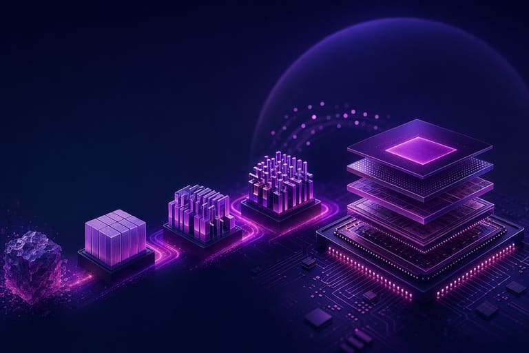
5nm மற்றும் குறை tech leaps pave way for the “2nm” chip era — smaller, faster, lesser power. EUV lithography, Gate-All-Around FET, advanced new material-கள்; fabrication-இல் பிறந்த engineering marvel-கள்.
| Technology | Transistor density (per mm²) | Expected launch | Features |
|---|---|---|---|
| 5nm | 171.3 million | 2020-2022 | High performance, low power |
| 3nm | 291 million | 2022-2023 | Better power efficiency |
| 2nm | ~450 million+ | 2024+ (Estimate) | Superperformance, energy savings |
| 1.4nm (Angstrom) | Unknown | 2027+ (Target) | Future extreme performance chips |
2nm chip progress: atomic-level control, EUV optimization, new transistor design, prototype, testing, mass production. Mobiles to datacenters — tomorrow’s tech leaps, engineering barrier breakthroughs, user magic! 5nm மற்றும் குறை chips; just “fast”— இல்லாமல், சேவை, device, intelligence எல்லைக்கும் முழுமையாக உருட்டும்.
5nm செயலிகள்: பயனாளர்கள் அறிய வேண்டியது
5nm chip mobiles, laptops-இல் real-world experience-ஐ மாற்றுகிறது. Smaller transistor — more power; lightning quick apps, smooth gameplay, general system responsiveness — “கண்ணில் பட்டவுடன்”.
Energy efficiency-ன் பயனாளர் “தீர்வு”: battery runtime lengthens — mobile use all-day, travel, power-cut even — plug-in worryless. Lesser heat, lifetime boost, system reliability leaps.
| அம்சம் | 5nm chip | Previous gen chip |
|---|---|---|
| Processing power | Higher | Lower |
| Power draw | Lower | Higher |
| Battery life | Longer | Shorter |
| Heating | Lesser | Greater |
பயனாளர் வரம்புகள்
- Apps lightning open; speedy multitasking
- Game smoothness; hi-res visuals
- All-day battery
- Low heating, stable device
- AI/ML powers expand
- Photo/video processing speed leaps
5nm chips-இல் AI, ML நுண்ணறிவு இரட்டிப்பு: Smart assistants, smart tools, photo editing, user experience-யை புதிய அளவுக்கு முன்னேற்றும். இவை, நாளைய கைபேசி, laptop, server உலகத்திற்கு அடித்தளம் அமைக்கின்றன.
நன்மைகள், சிக்கலான பக்கவிளைவுகள்
5nm மற்றும் குறை chip tech leaps: high density, higher performance, lesser energy — ஆனால் companion “tightrope”: fabrication cost, heat, quantum tunneling. இது engineering-க்கும், economy-க்கும் balance-ஐ யாரும் தவிர்க்க முடியாது.
- 5nm chip positives vs negatives
- நன்மைகள்:
- Higher processing power
- Lesser power usage
- Smaller device size
- Faster data
- Advanced AI & ML
- பத்தும் பக்கவிளைவுகள்:
- High manufacturing cost
- Complex design/fabrication
- Heating issues
- Quantum tunneling effect
- Ultra-precise production needed
- நன்மைகள்:
Performance spike, but fabrication “headache”— manufacturing cost, defects, overheating, electric interference; balancing act needed. But cooler innovation, EUV lithography, R&D, new materials — heat issues, defect rates overcome-ஆவது.
| அம்சம் | Positive | Negative |
|---|---|---|
| Transistor Density | Super-performance, more features | Complexity, defect risk |
| Power | Battery, energy saving | Thermal issues, heat sink needed |
| Cost | Value in flagship devices | High price, exclusive segment |
| Reliability | Advanced error-correction | Quantum impact, unpredictable behavior |
Material innovations, fabrication leaps, EUV lithography, efficient cooling overcome “headaches”. 5nm மற்றும் குறை chip progress — mobiles to datacenters, performance leaps, efficiency leaps, price-down trend-க்கு அடித்தளம் அமைக்கிறது.
முடிவு: 5nm தொழில்நுட்பத்தின் எதிர்கால பாதம்
5nm மற்றும் குறை chip progression — fast, efficient, powerful devices foundation. Massive transistor count small area, performance spike; mobiles, supercomputers, future innovation-க்கு வாயிலாகும். Engineering, fabrication, material hurdles-க்கு balance போட்டால்தான், leaps possible.
| Tech | நன்மைகள் | பக்கவிளைவுகள் |
|---|---|---|
| 5nm chips | Super performance, ultra-low power | High cost, complex design |
| 3nm chips (future) | Greater performance, even less power | Manufacturing hurdles, new materials |
| 2nm and below (research) | Outstanding potential, energy savings | Physical limits, unsolved technical roadblocks |
Future: not just consumer electronics — AI, autonomous vehicles, healthcare, everything influenced. Performance bridges: AI faster, autonomous safety, medical precision leap. 5nm tech key moves
- Research/Development investment up
- Material innovation — silicon alternatives
- Fabrication cost/time breakthroughs
- Global engineering cooperation
- Skilled workforce, STEM focus
Future leverage: fabrication cost reduction, physical limits breach, new material integration — industry-opportunity. 5nm மற்றும் குறை chips, tomorrow’s technology stepping stone.
5nm technology isn’t just “next”; it’s the foundation stone for future innovation.
Nanometer chip leaps = smarter, faster, greener devices; life-changing moves. Investment, R&D, skilled engineering — leadership for tomorrow.
நடவே! 5nm மற்றும் குறை செயலிகளுக்கான நடைமுறை அறிவுரை
5nm மற்றும் குறை chip investment, usage consider-ஆட்டீர்கள் என்றால், aspect analysis — power, performance, cost, application-specific planning key. Mobile-க்கும் battery life, servers-க்கும் speed — architecture, features-க்கு priority!
Software, algorithm optimization — real world benefit; parallel compute, AI, ML leverage. Compiler tuning, low-level optimization — chip resource smart utilization; performance leaps!
| Step | Explanation | Recommended actions |
|---|---|---|
| 1 | Needs analysis | Set power, speed, cost criteria |
| 2 | Architecture selection | Choose CPU design (ARM, RISC-V, etc) suited for your app |
| 3 | Software optimization | Parallel processing, compiler tweaks, low-level code |
| 4 | Cooling solutions | Use best thermal management for high-performance chips |
5nm மற்றும் குறை chips, high transistor density = more heat. Intelligent cooling: advanced heat spreader, liquid cooling, or smart power management; prevent overheating; preserve speed, longevity!
Implementation tips
- Use latest dev tools/libraries
- Performance profiling bottleneck checks
- Dynamic frequency scaling (DFS) for power savings
- Optimize memory access for speed
- AI apps — hardware acceleration for best results
5nm tech constantly evolving. New architectures, materials, production methods — tomorrow even greater leaps. Stay tuned, optimize, maximize potential! Strategy, optimization — 5nm அல்லது குறை chip leaps unlock everything.
அடிக்கடி கேள்விகள்
5nm மற்றும் குறை chip tech, real world-ல் எப்படி பயன்?
Smaller chips = more transistors on die = faster processing, low power, long battery. Direct user benefit: fast apps, smooth games, responsive devices.
சிப்சில் புதிய பொருட்கள், ஏன் அவசியம்? எந்த engineering தடைகளை தாண்டும்?
Silicon constraints breached; novel materials = faster electrons, better heat dissipation, low power; energy-efficient chips. Quantum tunneling, leakage issue overcome-ஆறும்.
2nm chip fabrication hurdles: எப்படி engineering-ல் வேலைபார்க்கப்படுகிறது?
Atomic precision, quantum limits, new lithography, innovative transistor design; AI/ML optimise fabrication, prototype design/testing, overcome.
5nm மற்றும் கீழ் chip fabrication cost—பயனாளர் impact? Price always high?
Production cost leap, device price hike; but performance, battery life, user-experience offset. Entry-level device widespread takes time.
ARM, x86 architectural impact—5nm மற்றும் அதற்கும் கீழ் integration-ல் வேறுபாடு?
Both architectures leverage 5nm advancements. ARM focuses power savings, x86 raw performance. Differences in efficiency, workload type.
Quantum tunneling — 5nm chip limitation, engineering ‘defense’?
Quantum tunneling: electrons leaking when transistors “closed”; effect stronger as size shrinks. High-K metal gate (HKMG), innovative design, fabrication tech limit leaks.
5nm chip device — எல்லையிலும் மட்டும் பார்த்தால் போதும்? வேறு factors?
Just chip size insufficient; architecture, cores, clock, RAM, cooling, software optimization, use-case matter. Check reviews, benchmarks, user feedback.
Environmental impact — energy savings, sustainability?
Low-power chips = carbon footprint cut. Battery life up, fewer charges, less waste. Responsible production, green methods important — sustainability key.